Curators approve Missouri S&T semiconductor engineering program
Posted by Greg Edwards
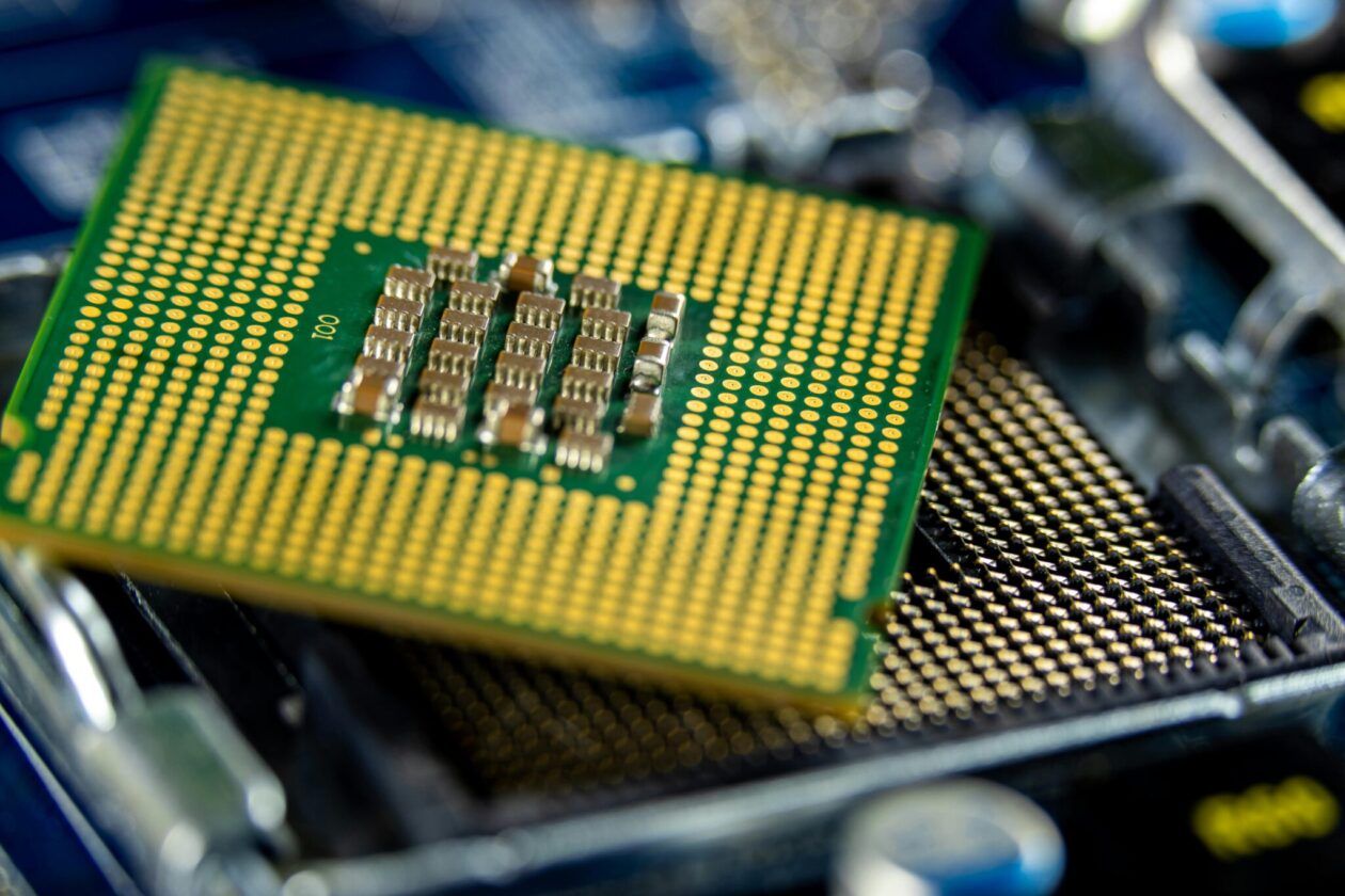
An integrated circuit, or computer chip, contains billions of tiny semiconductor devices that are used to perform calculations and other tasks. Photo by Sergei Starostin.
The University of Missouri Board of Curators unanimously voted today (Feb. 6) to approve a new bachelor’s degree program in semiconductor engineering at Missouri S&T.
“We are grateful to the curators for recognizing the importance and urgency of launching this program — not just for our state, but for the entire nation,” says Dr. David Borrok, vice provost and dean of the S&T College of Engineering and Computing. “Projections show the semiconductor engineering profession’s workforce gap is on track to be in the tens of thousands in the coming years, and Missouri S&T is ready to help meet this need.”
The 128-credit-hour program was made possible thanks to a $20 million investment from private sources. Part of this investment will allow students to learn and apply their skills in a new 2,500-square-foot cleanroom located on the ground floor of S&T’s Applied Research Center, which should be ready for use by late 2026.
Students will be able to choose between two emphasis areas — semiconductor device engineering and semiconductor process engineering.
“All students will gain extensive hands-on experience with semiconductor materials processing, as well as microelectronics device fabrication and testing in industry-relevant cleanroom environments,” says Dr. David Lipke, an S&T associate professor of materials science and engineering. “Then, they will further specialize in one of these areas to better prepare them for key positions in modern semiconductor foundries and related technology fields.”
Lipke says the new program will be housed in the S&T materials science and engineering department, but because it will be interdisciplinary, it will also feature classes in S&T’s electrical and computer engineering department and the Linda and Bipin Doshi Department of Chemical and Biochemical Engineering.
“Semiconductor engineers require technical knowledge, skills and abilities from multiple fields of engineering,” Lipke says. “But that’s the great thing about Missouri S&T. We have nationally recognized engineering programs in each of these areas and therefore provide students with an exceptional hands-on education.”
Pending approval from the Missouri Coordinating Board for Higher Education, the university plans to offer the degree program starting in fall 2025.
To apply for Missouri S&T’s semiconductor engineering program, visit apply.mst.edu. More information is available at go.mst.edu/semiconductorengineering.
About Missouri S&T
Missouri University of Science and Technology (Missouri S&T) is a STEM-focused research university of over 7,000 students located in Rolla, Missouri. Part of the four-campus University of Missouri System, Missouri S&T offers over 100 degrees in 40 areas of study and is among the nation’s top public universities for salary impact, according to the Wall Street Journal. For more information about Missouri S&T, visit www.mst.edu.
Posted by Greg Edwards
Leave a Reply
 Sports Headlines
- Miners Lead Division II with Five At-Large CSC Academic All-Americans; Four from Men's Volleyball
- Miners Swim Earns 26th Consecutive Team Scholar All-America; Six Individuals Also Honored
- Edmonds and Fraser Earn GLVC Scholar-Athlete Honors
- Miners Set School Record with 48 Council of Presidents’ Academic Honors
- S&T Sets New Department Standard for Br. James Gaffney Distinguished Scholar Honorees
Good to read about the new semi-conductor program. Very timely and appropriate! I suggest publishing an article about this addition in at least the St. Louis and KC newspapers.