Atomic-layer electrodeposition method yields surprising results
Posted by Andrew Careaga

Dr. Jay A. Switzer
A new method for creating very thin layers of materials at the atomic scale, reported in the latest issue of the journal Science, could “unlock an important new technology” for creating nanomaterials, according to nanomaterials expert Dr. Jay A. Switzer of Missouri University of Science and Technology in the journal.
Switzer was asked by the editors of Science to discuss the research, which identifies a new method of atomic-layer deposition (ALD), in the “Perspectives” section of Science. The research and Switzer’s Perspective article both appear in the journal’s Dec. 7, 2012, issue.

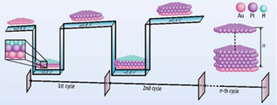
This illustration depicts how atomic-layer electrodeposition of ultrathin platinum films is achieved through a new process discussed by Missouri S&T Professor of Discovery Jay A. Switzer.
The research by Dr. Yun Liu and colleagues at the National Institute for Standards and Technology’s Center for Neutron Research describes a new method for depositing ultra-thin layers of platinum on a surface. The method involves applying a “high overpotential” of electricity to deposit a layer of the metal on a surface, then to toggle to an underpotential to produce a layer of hydrogen. The hydrogen remains in place only briefly, then disappears as scientists adjust the voltage to add new layers of platinum.
The approach yields unexpected results, Switzer says.
“Conventional wisdom would suggest that the best way to electrodeposit ultra-thin metal films would be to apply either an underpotential or a very small overpotential,” writes Switzer, an expert on atomic-layer depositions. Liu and his colleagues “report the surprising result” that a single layer of platinum, placed on the surface at a voltage that should create a thick deposit of the metal, actually creates the layer of hydrogen that limits the thickness of the platinum layer, “thereby making the process self-limiting.”
“The beauty of this new electrochemical route to ALD is that it blends basic electrochemistry and surface science to unlock an important new technology,” says Switzer, who is the Donald L. Castleman/Foundation for Chemical Research Professor of Discovery at Missouri S&T.
Atomic-layer electrodeposition is a method of “growing” materials in a solution at the nanometer-scale. A nanometer – visible only with the aid of a high-power electron microscope – is one billionth of a meter, and some nanomaterials are only a few atoms in size.
Liu’s discovery could result in a new method for growing metal oxides or semiconductors at the atomic scale, Switzer says. “The prospects of this as a general processing method (for atomic-scale deposition) are encouraging,” he writes.
Leave a Reply